Version used: Altium 17
Let's focus at our propose "Creating a single layer board fast and within an outstanding quality". Now is time to introduce one of our guiding files "Best Practices for PCB Design for World Skills Competitors". Take a general look, we'll constantly look at it.
You should be at the 11th step from our guide and all the previous steps were successfully finished.
----------------------------------------------------------------------------------------

As we only have one layer, all SMD components must be at the bottom layer. Select them and at the PCB Inspector change the Layer to Bottom Layer.
----------------------------------------------------------------------------------------

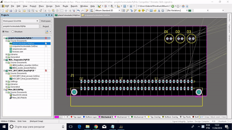
Start moving to the board your interface components. For example connectors, LEDs, buttons, switches, etc. Normally you already have a position for those components considering it will interact with something or someone in real life.
----------------------------------------------------------------------------------------

To avoid messing up with those components is a good idea to lock them.
Select them all, open the PCB Inspector and click "locked"
----------------------------------------------------------------------------------------
Right click at your schematics tab and -> Open in new window.
If you have two monitors split your work project to see Schematics in one monitor and PCB in the other.
If you don't have two monitors (buy a second one) use Alt+tab to swap windows faster.
----------------------------------------------------------------------------------------

Now at your Schematics, be sure the Cross selection tool is active, click Tools->Cross Select Mode
----------------------------------------------------------------------------------------
As our best practice number 6 advice, you must separate your project into subgroups, it will avoid long traces when you start routing. At this point only experience will make you understand where is the best place to start, but as a general rule for beginners, follow the signal flow.
Start by the input, select some components in your schematics. Go to your pcb window (Alt+tab or click in the PCB monitor) and press t+o+l then select the area you want to move your selected components.
----------------------------------------------------------------------------------------
Look at the net lines and move and rotate your components until find some position where your net lines are shorter and less crossed.
----------------------------------------------------------------------------------------
After finishing the placement of this first group go back to your schematics, select more components (following your circuit flow) and at your PCB press t+o+l again.
Repeat this process over and over again, until placing all components.
TIP: If you select a smaller number of components will be easier to organize them.
TIP2: Do not start to trace here yet, finish all your placement first, then start routing. You'll notice that when your project is big you'll need to move your blocks around to avoid empty spaces.
TIP3: As you decide where to put your components based on net lines, sometimes the GND net disturbs more than help so you can hide it clicking View->Connections->Hide Net and clicking at the GND. As we'll create a GND plane, you don't need to mind about GND connections at this point.
TIP4. Now is the best time to double check your packages. While placing stop looking at the PC screen sometimes and look at your actual parts to see if you have chosen the right footprint.
Attention: Be careful! Do not place plastic components near to other that heats up.
Attention2: Do not place tall components near buttons or other interface component that may be hard to access if some tall component is near by.
No comments:
Post a Comment